Advanced Capabilities, Your Trusted Partner

Corporate History

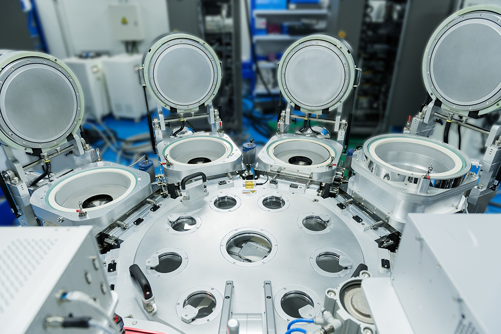
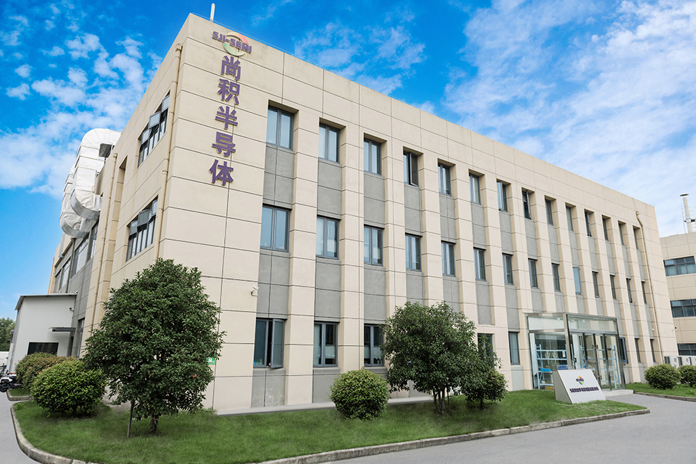
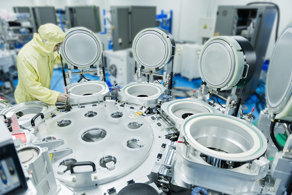
SJI-SEMI Co.,Ltd is a China-based semiconductor equipment manufacturer specializing in metal sputtering deposition (PVD), plasma enhanced chemical vapor deposition (PECVD), plasma dry etching (ETCH) systems and serving for the Power Devices, MEMS, Advanced Packaging, III-V and RF Compound Semiconductor, and IC customers in the world. The equipment has excellent repeatability and stability, low failure rate, long service life and easy operation and maintenance, and been widely recognized by customers.

SJI-SEMI are well-known on providing Vanadium oxide (VOx/VO2), TC-SAW SiO2 and high vacuum inspiratory Getter thin film depositions on MEMS market and the key processes of Thin Film Resistors on RF market such as TaN thin film deposition. The technical results and performance of those thin film depositions are way beyond the imported equipment’s and have been manufactured in the mass production lines at the customer sites. Our market share of those thin film depositions is far ahead

On Power Device market, SJI-SEMI are also famous on the front-side metal (FSM) Hot Al films sputtering by its excellent high AR hole-filling ability and planarization capability, and the AR ratio up to 3.5:1 @ 0.2um Bottom CD, is surpassing the imported equipment; in addition, SJI-SEMI’s back-side metal films sputtering (BSM) has stable performance and its productivity is nearly twice of the imported equipment’s, especially in the SiC power industry, our market share of FSM Hot Al and BSM is far ahead too.

With more than 20 years of experience in the IC industry, we have deep and diversified knowledge in many techniques such as high AR hole-filling, uniformity optimization, stress control, diversity and complexity of thin films.

Also, SJI-SEMI’s PECVD and ETCH equipment can directly replace the imported equipment in the MEMS, RF, Power and other semiconductor fields, and offer better process solutions.

Values

SJI-SEMI——Pragmatic, Active and Progressive

Visions

To become a world-class integrator of semiconductor vacuum equipment and advanced processes.

Missions

Being a professional local semiconductor vacuum equipment supplier to focus on the substitution of core equipment and key process solutions in the semiconductor industry, and actively seek and deploy new technologies to be a technology leader.

Corporate History

In 2008, the team entered the field of MEMS

In 2008, the team entered the field of MEMS -- In 2008, the team entered the field of MEMS and developed Vanadium Oxide thin film sputtering, penetrating the foreign technology monopoly and taking a far leading market share.

In 2012, the team developed the high vacuum inspiratory Getter

In 2012, the team developed the high vacuum inspiratory Getter thin film sputtering -- in 2012, the team developed the high vacuum inspiratory Getter thin film sputtering, penetrating the foreign technology monopoly again, and being the local semiconductor equipment supplier in China for the process with a far leading market share as well.

In 2019, the team entered the field of Power Devices

In 2019, the team entered the field of Power Devices -- In 2019, the team entered the field of Power Devices and developed Hot AI hole-filling process for metal thin film sputtering, becoming the first local equipment supplier for this process in China with a far leading market share once again.

In 2020, the team developed the SiC backside metal thin film sputtering

In 2020, the team developed the SiC backside metal thin film sputtering -- In 2020, the team developed the SiC backside metal thin film sputtering BSM, becoming the first local equipment supplier for this process in China.

In 2021, the team developed Si back-side metal thin film sputtering

In 2021, the team developed Si back-side metal thin film sputtering -- In 2021, the team developed Si back-side metal thin film sputtering, becoming a rare local equipment supplier for this process in China with better performance than the local peer equipment suppliers’.

In 2021, the team developed TaN Lift Off thin film sputtering in the field of RF, becoming a rare local equipment supplier for this process in China.

In 2022, the team developed the TC-SAW SiO2 thin film sputtering in the field of RF Filter

In 2022, the team developed the TC-SAW SiO2 thin film sputtering in the field of RF Filter -- In 2022, the team developed the TC-SAW High-Dense SiO2 thin film sputtering in the field of RF Filter, becoming a rare local equipment supplier for this process in China too.

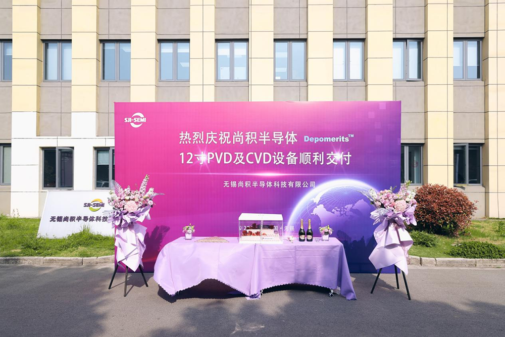
In 2024, the team developed the 300mm PVD and CVD

In 2024, the team developed the 300mm PVD and CVD

Core Team

SJI-SEMI Co.,Ltd independently cultivates and incubates our own core team with an average working experience of more than 20 years. They have been deeply involved in the semiconductor equipment industry for a long time with local and overseas work backgrounds, forward-looking international vision and industry chain resources for equipment manufacturing.